
Simplifying Innovation in Microelectronics with Multi-Material Laser Machining
Client & Industry Context
Microelectronics continue to trend smaller, lighter, and more complex. Engineers and manufacturers in this space are under constant pressure to innovate — not only by shrinking component dimensions, but also by ensuring consistent performance across a variety of materials. Achieving this level of precision is critical for applications such as printed circuit boards (PCBs), semiconductor packaging, and high-performance electronic assemblies.
The Challenge: Consistency Across Materials
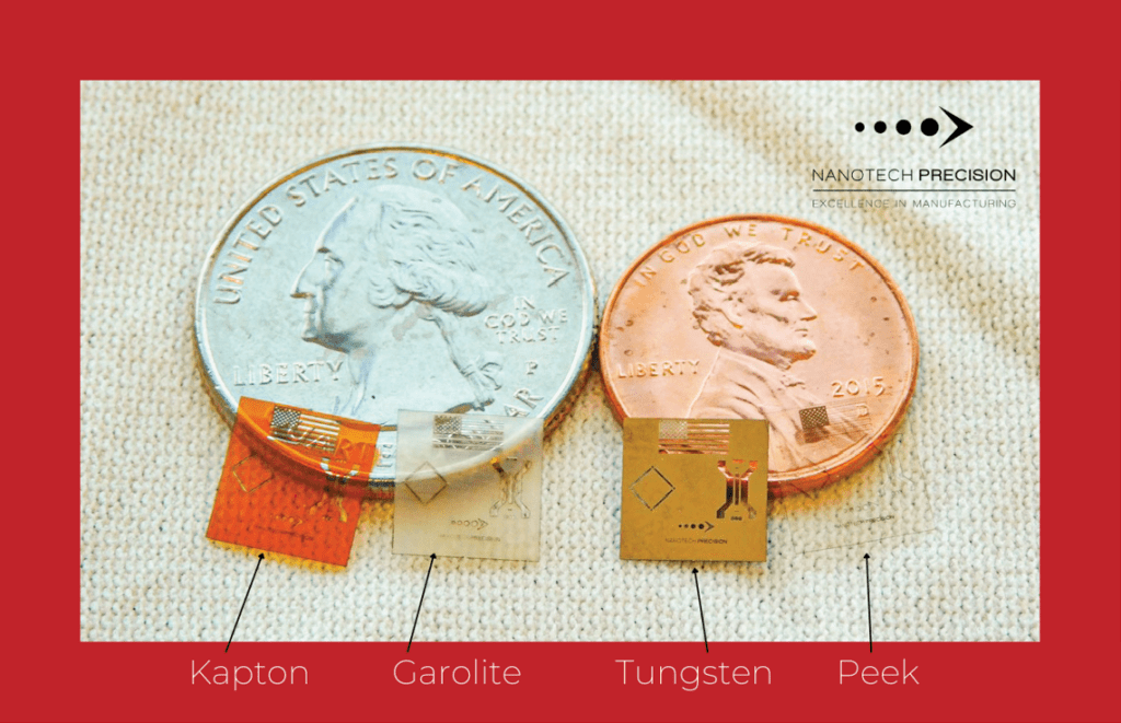
As products grow more sophisticated, design requirements often demand the use of diverse materials — from polymers to metals — each with unique machining characteristics. Traditional processes struggle to deliver consistent micro-scale results when switching between substrates like Kapton, Garolite, Tungsten, and PEEK. The challenge was clear: demonstrate the ability to achieve identical designs across a wide range of materials without sacrificing precision or repeatability.
Nanotech’s Solution: Femto Laser Versatility
Nanotech Precision turned to its Femto Laser System, leveraging its unparalleled stability and precision to machine a single microcircuit design in four distinct materials:
Kapton (polyimide film, widely used in PCBs)
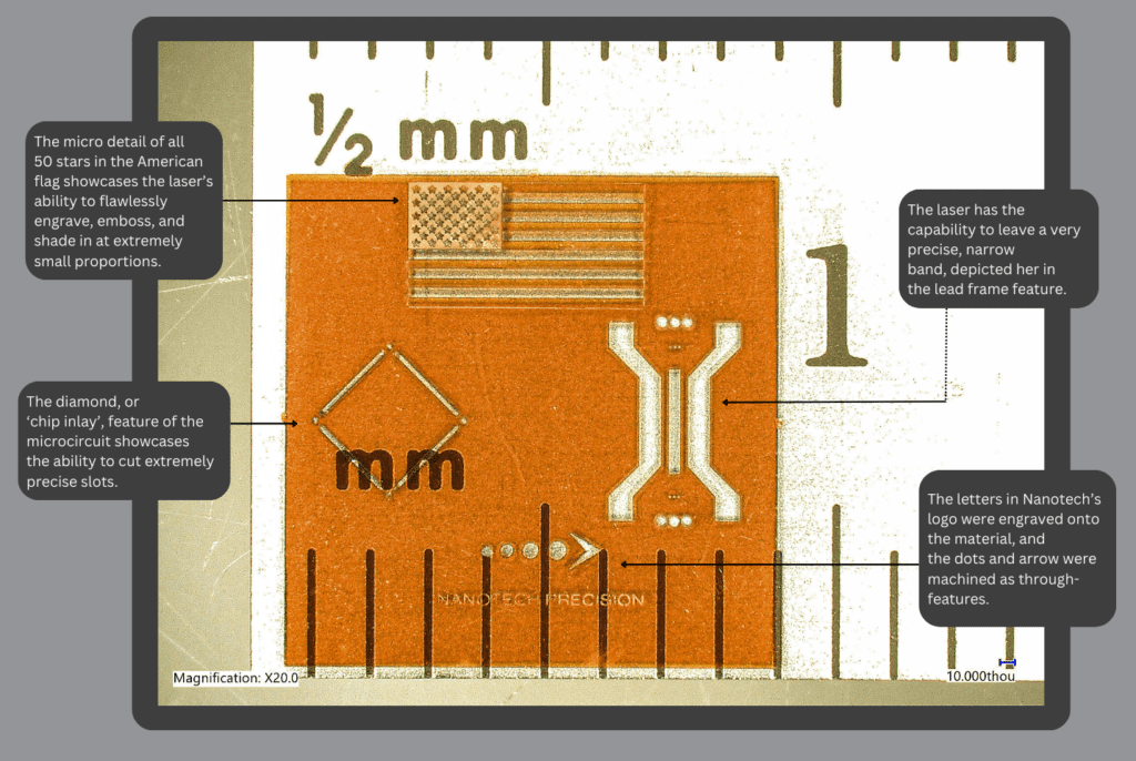
The micro detail of all 50 stars in the American flag feature showcases the laser’s ability to flawlessly engrave, emboss and shade in at extremely small proportions. The diamond, or ‘chip inlay’ feature of the microcircuit showcases the ability to cut extremely precise slots. The laser has the capability to leave a very precise, narrow band, depicted here in the lead frame feature. The letters in the logo were engraved onto the material and the dots and arrow were machined as through-features.
Garolite (high-strength composite laminate)
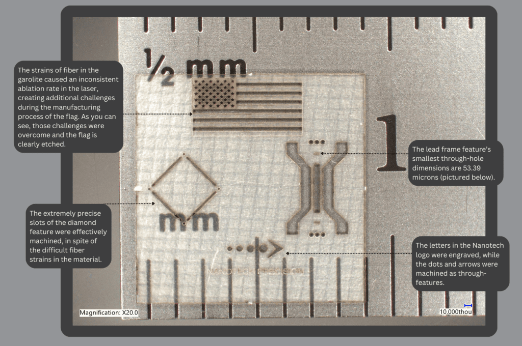
The strains of fiber in the garolite caused an inconsistent ablation rate in the laser, creating additional challenges during the manufacturing process of the flag. In spite of the difficult fiber strains in the material, the extremely precise slots of the diamond feature were effectively machined. The lead frame feature’s smallest through-hole dimensions are approximately 53 microns.
Tungsten (transition metal, valued for conductivity and durability)
This metal proved to be the least problematic material to machine. Zero cutting force from the laser provides the ability to successfully machine these compact features. All 50 stars were neatly shaded in, while the narrow stripes of the flag were kept sharply in tact. The smallest features in the lead frame have roughly the same diameter as a human hair.

PEEK (high-performance thermoplastic polymer)
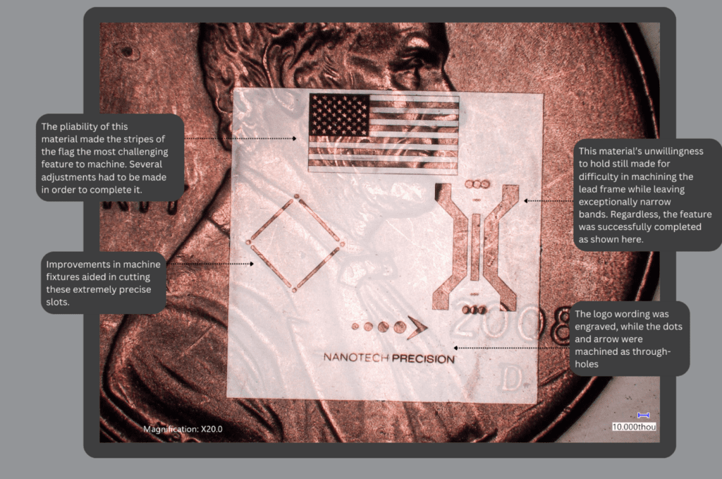
The pliability of this material made the stripes of the flag the most challenging feature to machine; several adjustments had to be made in order to complete it. Improvements in machine fixtures aided in cutting these extremely precise slots. The material’s unwillingness to hold still made for difficulty in machining the lead frame while leaving exceptionally narrow bands.
Each microcircuit was produced with identical geometry, proving the Femto Laser’s ability to handle both polymers and metals with equal precision. The laser’s ultrashort pulses eliminated thermal stress and material distortion, ensuring clean edges, sharp features, and uniform results across all substrates.
Results & Impact: Reliable, Repeatable Microcircuits
The demonstration successfully showcased four finished microcircuits, each identical in design but manufactured from very different materials. The results highlight:
- Design flexibility: Engineers can now explore wider material options without compromising manufacturability.
- Precision repeatability: Micron-level accuracy was maintained across all four substrates.
- Broader applications: The solution applies directly to PCB manufacturing, microelectronics, and high-density circuit design.
This proof-of-concept confirms that material constraints no longer limit innovation — paving the way for faster, more versatile product development.
Why Nanotech Precision: Making Small Simple
Nanotech Precision is committed to simplifying the path to innovation in microelectronics. By combining high-volume production expertise with femtosecond laser technology, we help engineers achieve micro features that were once considered impractical. Our ability to deliver consistent, high-quality results across multiple materials sets us apart as a partner in next-generation microelectronics manufacturing.
Ready to get started?
Get In Touch
Join Our Team!